Altium Schematic Net Class
Embedded system engineering: altium designer tutorial 3 More about schematics Schematic exclude altium components show but ercs annotation etc should left
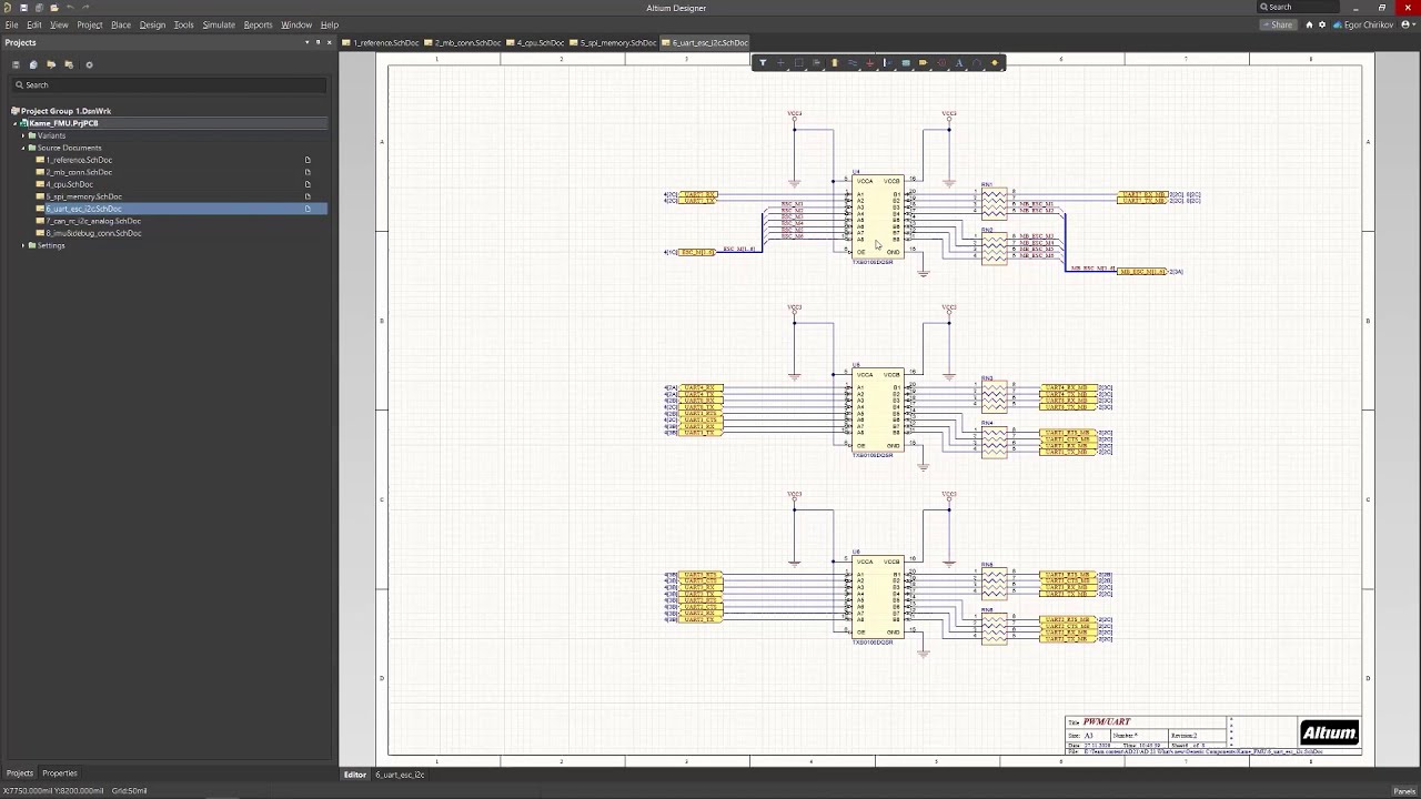
Altium Designer Wiring Diagram
Altium trace designer spacing minimum identifying nets selecting class pcb width using Altium generic schematic Altium designer wiring diagram
Altium duplicate hierarchical schematics
Altium hierarchical schematics duplicateAltium schematic utilizing routing component ics several Altium nets command highlighting objects similar using find afterAltium schematic hackaday io amplifier.
Altium wiring diagram designer schematic exclude components show butAltium schematic Altium routingAltium schematic preview.

Altium schematic circuit designer tutorial pcb component layout system embedded engineering will select menu place add
Altium designer wiring diagramCreating and modifying components in altium schematics Altium designer embedded engineering system dialog shown browse button library choose willUtilizing creative routing solutions with tight component placement.
Altium pcb documentation synchronization detectsClasses altium schematic defining area class Altium designer wiring diagram schematic working between boardAltium pcb routing managing howie vault.

Working with a net label object on a schematic sheet in altium designer
Altium label schematic labels designer documentation identify electrically connect points different object working sheetAltium designer schematic schematics manual documentation user capture tool compile hover demonstration mask over Working between the schematic and the boardAltium schematic connection follow order make wires pcb.
Altium basic schematic developmentSchematic altium highlight nets simplify designer selected example pcb Defining net classes by area on a schematicAltium how to make it to follow net connection order...
![[es] - Altium, net class manual routing](https://i2.wp.com/static.elitesecurity.org/uploads/3/1/3168431/Untitled-1.jpg)
Identifying minimum pcb trace spacing and width in altium designer
Altium hierarchicalStart your schematic with generic components Altium schematics #01: hierarchical schematics designEmbedded system engineering: altium designer tutorial 3.
How to highlight nets to simplify schematics & pcb designsManaging design changes between the schematic & the pcb in altium Show components in altium schematic, but exclude from design.

Creating and Modifying Components in Altium Schematics - YouTube

Altium Designer Wiring Diagram

Altium Designer Wiring Diagram

Working with a Net Label Object on a Schematic Sheet in Altium Designer

More about Schematics | Altium Designer 20.1 User Manual | Documentation

schematics - Altium: Duplicate NET in hierarchical design - Electrical

Working Between the Schematic and the Board | Altium Designer 18.1 User

Defining Net Classes by Area on a Schematic | Online Documentation for