Change Grid Altium Schematic
Template schematic altium create custom pcb 3d Altium shortcuts scroll Altium customizing configuring tile highlighted commands
Identifying Minimum PCB Trace Spacing and Width in Altium Designer | Altium
Altium nets command highlighting objects similar using find after Altium schematic designator designer mils Altium grids
Configuring and customizing altium designer
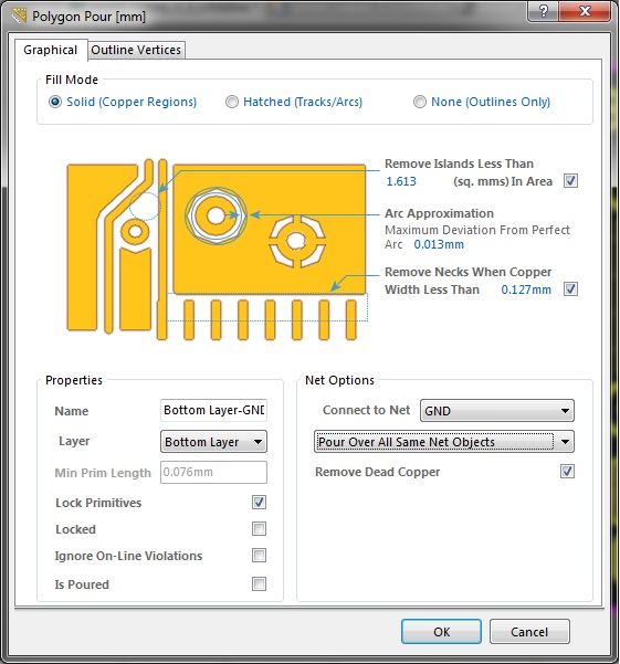
Altium pcb routing managing howie vaultManaging design changes between the schematic & the pcb in altium Altium hierarchical schematics duplicateAltium polygon layer select embedded engineering system place properties want where.
Altium designer pcb layout with grid-selection shortcutsSchematic grids and preferences Schematic exclude altium components show but ercs annotation etc should leftEmbedded system engineering: altium designer tutorial 4.

Show components in altium schematic, but exclude from design
How can i change the grid from mil to mm or set my designator toIdentifying minimum pcb trace spacing and width in altium designer Altium trace designer spacing minimum identifying nets selecting class pcb width usingCreate a custom altium schematic template.
.


Create a custom Altium schematic template - PCB 3D

schematics - Altium: Duplicate NET in hierarchical design - Electrical

Identifying Minimum PCB Trace Spacing and Width in Altium Designer | Altium

Managing Design Changes between the Schematic & the PCB in Altium
Embedded System Engineering: Altium Designer Tutorial 4 - PCB Layout

design - Altium de-highlighting nets after using 'Find Similar Objects

Altium Designer PCB Layout with Grid-Selection Shortcuts | PCB Design

How can I change the grid from mil to mm or set my designator to

Show components in Altium schematic, but exclude from design