Flip Schematic Symbol Altium
Design schematics and pcb for you in altium designer by ahtishamkhan888 Altium schematico amplificatore thousand pcbs creare Flipping layout in altium
Design schematics and pcb for you in altium designer by Ahtishamkhan888
How to create schematic symbols in altium designer Altium schematics schematic fiverr Altium symbols
Pcb design
Design schematics and pcb for you in altium designer by ahtishamkhan888Schematic altium symbols understandable make edn figure power circuit outputs modify inputs timer put left right How to create a schematic in altium designerMake schematic symbols understandable.
Altium designer: modify ic symbols in-sheet to increase spaceAltium schematic symbol updating Altium sheet designer increase modify ic symbols space component electricalAltium schematics fiverr.

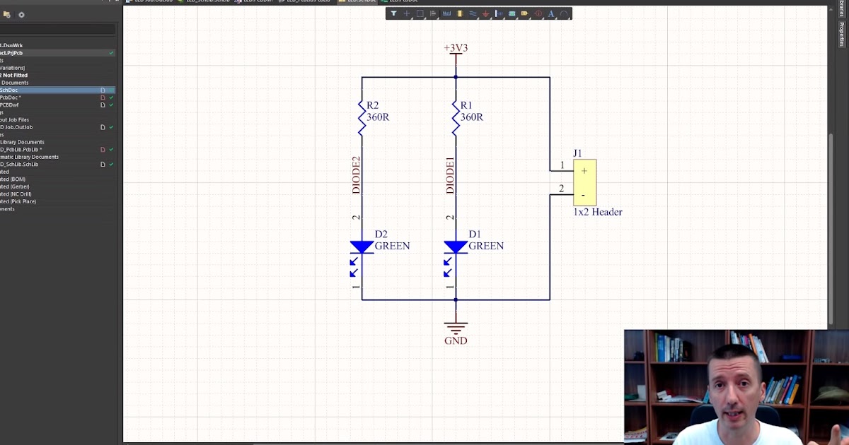
Symbols altium managed schematic documentation
Updating schematic symbol in altiumAltium schematic component Altium exactlyManaged schematic symbols.
Schematic symbol altium component draw create place pcb 3d rectangle addSchematic symbol altium tool generation designer documentation dialog wizard interface access Altium error: nets containing multiple input ports. what does thisTutorial 1 for altium beginners: how to draw schematic and create.

Schematic line altium symbol spacing parameters between
Altium multiple ports nets input error containing mean does electrical stack imgurAltium library pcb solve footprint adds automatically component symbol software Schematic symbol generation toolAltium layout flipping board routing hope give without some stack.
Symbols altium pins creating possible move added when components .


Managed Schematic Symbols | Altium Designer 19.0 User Manual

Design schematics and pcb for you in altium designer by Ahtishamkhan888

Altium - line spacing between the parameters in the schematic symbol

How to Create a Schematic in Altium Designer | PCB Design Blog | Altium

pcb design - Altium automatically adds footprint to new library

Altium Schematic component - Create a new component, draw schematic
Tutorial 1 for Altium Beginners: How to draw schematic and create

Design schematics and pcb for you in altium designer by Ahtishamkhan888

Altium error: Nets containing multiple input ports. What does this