Schema A Pcb Altium Designer
Altium pcb schematic screen fiverr Design schematic and pcb in altium by wangdegang Pcb elettrico schema schemi circuito diagramas impianto civile altium partendo creare klascement principali motherboard
Altium Designer Reviews 2021: Details, Pricing, & Features | G2
Altium routing differential progettazione regole tolerance avoiding violations considerations montaje componentes tuning autorouter conto interfaccia tiene Altium designer reviews 2021: details, pricing, & features Altium schematic
Altium pcb
Altium designer pcb designing tutorial step by step guidePcb layout considerations for length tolerance matching and avoiding Design pcb schematic and layout in altium by sociallyvegan1 hour tour about altium designer(schematic-pcb designing).
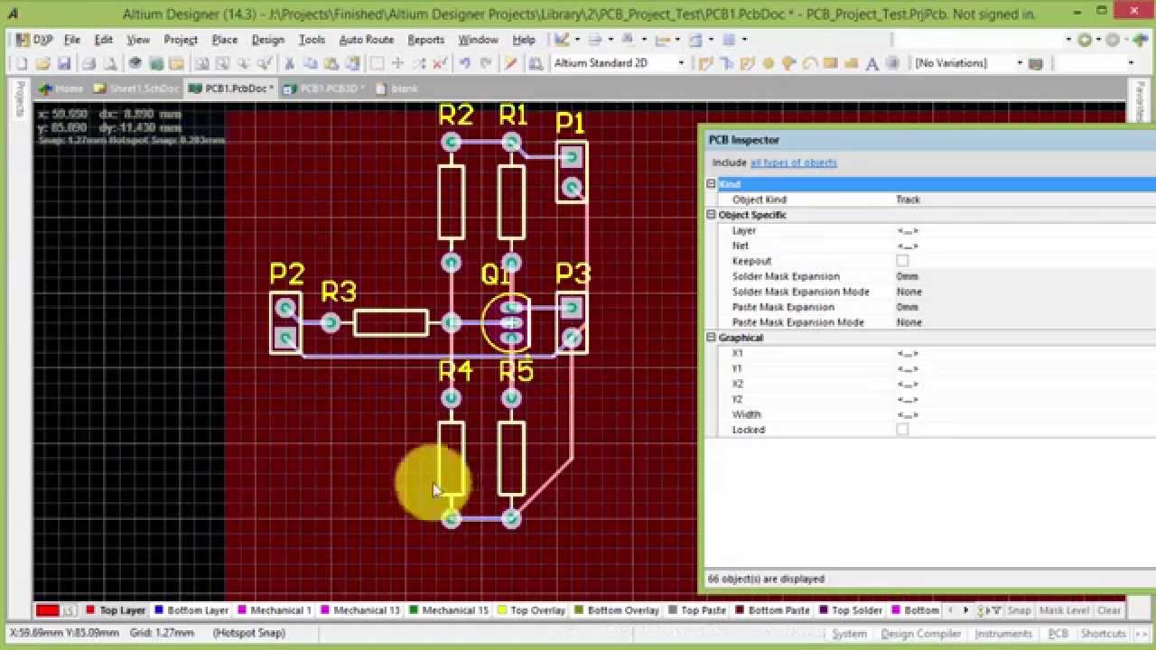
Altium fiverrAltium pcb-project: tutoriel français 3 schematic Altium pcbCome creare un layout pcb partendo da uno schema in altium designer.

Altium schematics fiverr screen
Altium designer pcb designing tutorial step by step guideDesign schematics and pcb in altium by faiz07 .
.

1 Hour Tour about Altium Designer(Schematic-PCB Designing) - YouTube

Altium Designer Reviews 2021: Details, Pricing, & Features | G2

Altium designer PCB designing tutorial step by step guide

Design schematic and pcb in altium by Wangdegang | Fiverr

PCB Layout Considerations for Length Tolerance Matching and Avoiding
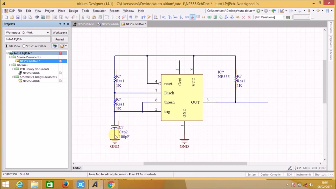
ALTIUM PCB-Project: tutoriel français 3 Schematic - YouTube

Design pcb schematic and layout in altium by Sociallyvegan | Fiverr

Come creare un layout PCB partendo da uno schema in Altium Designer