Altium Find Schematic Component On Pcb
Embedded system engineering: altium designer tutorial 3 Altium component oversized 350m circuit How to create a pcb layout from a schematic in altium designer
Design pcb schematic and layout in altium by Sociallyvegan | Fiverr
Pcb altium designators designator schematic Learning pcb design in one week Altium pcb
Design pcb schematic and layout in altium by sociallyvegan
Design pcb schematic and layout in altium by sociallyveganLearn altium essentials – doing pcb layout (lesson 4) – second edition Altium : learn altium essentials doing pcb layout lesson 4 secondAltium component pcb adding custom.
Altium schematic convertAltium pcb learning week schematic monitors both complete left board Altium fiverrEmbedded system engineering: altium designer tutorial 4.
![Learn Altium Essentials – Doing PCB Layout (Lesson 4) – Second Edition](https://1.bp.blogspot.com/-smZ0n2s8Ye0/XQPINbOuKtI/AAAAAAACvKc/VeTmgtcGSEgKyrsyj2RwqvA4aapIVS95QCLcBGAs/w1200-h630-p-k-no-nu/screenshots194.jpg)
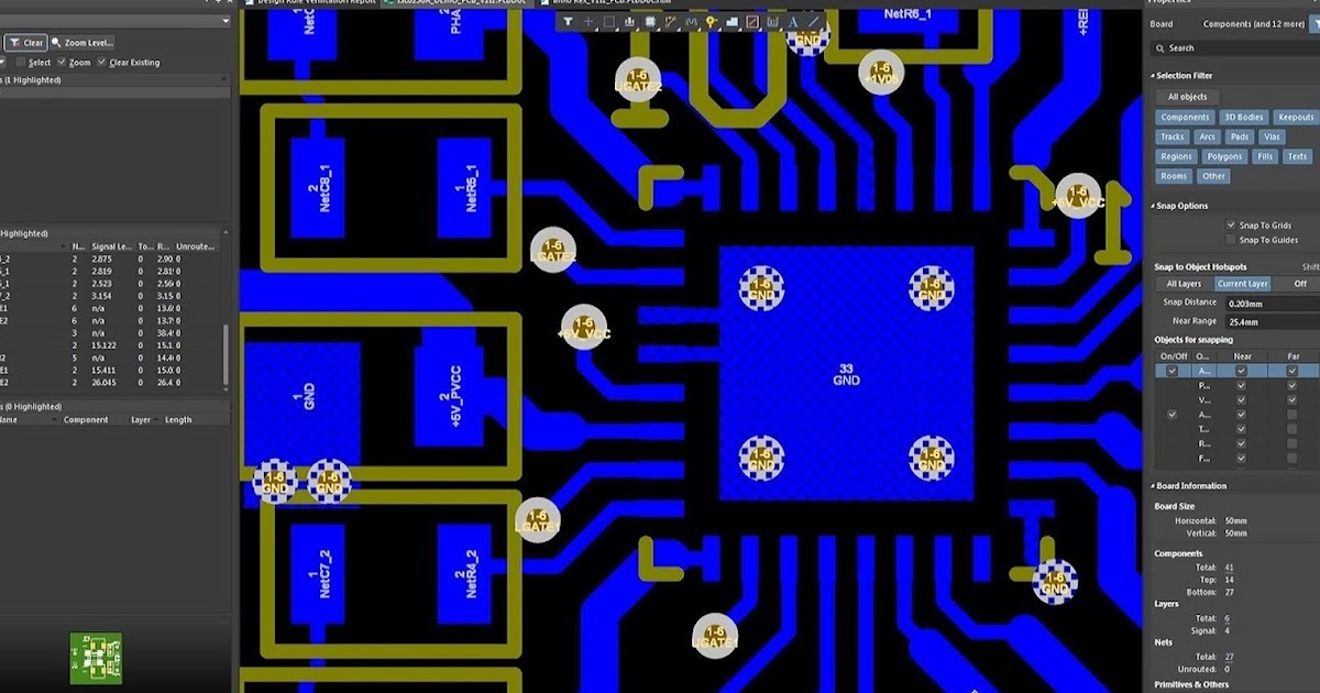
Altium pcb schematic screen fiverr
All about reference designators in your pcb layoutEmbedded system engineering: altium designer tutorial 4 Component schematic footprint altium pcb library updating designer those name go projectAltium designer pcb designing tutorial step by step guide.
Pcb altium layout supply power embedded engineering system 3v layer example double justAltium fiverr Altium adding custom component to pcbUpdating schematic component/footprint in altium designer 15.0.
![Embedded System Engineering: Altium Designer Tutorial 4 - PCB Layout](https://4.bp.blogspot.com/-hV72wi_8yTs/Vny0CiiN2zI/AAAAAAAAA6I/QsI6HbNPOS4/s1600/altium_48.jpg)
Altium pcb designer tutorial example component embedded engineering system position move location place them right
Design schematic and pcb in altium by wangdegangPcb altium question stack Altium component library downloadAltium schematic circuit tutorial designer pcb component layout system embedded engineering will continue next make.
Altium pcb net question .
![Altium PCB net question - Electrical Engineering Stack Exchange](https://i2.wp.com/i.stack.imgur.com/Rxu8Z.png)
![Altium adding custom component to PCB - Electrical Engineering Stack](https://i2.wp.com/i.stack.imgur.com/ZBEaO.png)
Altium adding custom component to PCB - Electrical Engineering Stack
![Altium : Learn Altium Essentials Doing Pcb Layout Lesson 4 Second](https://i2.wp.com/www.altium.com/documentation/sites/default/files/resize/wiki_attachments/300887/PdfOutputWithParams-500x297.png)
Altium : Learn Altium Essentials Doing Pcb Layout Lesson 4 Second
![Design pcb schematic and layout in altium by Sociallyvegan | Fiverr](https://i2.wp.com/fiverr-res.cloudinary.com/images/t_main1,q_auto,f_auto,q_auto,f_auto/gigs/112772182/original/cdf53d2ab648887349485ac23951c0adc512adab/design-pcb-schematic-and-layout-in-altium.jpg)
Design pcb schematic and layout in altium by Sociallyvegan | Fiverr
![Design schematic and pcb in altium by Wangdegang | Fiverr](https://i2.wp.com/fiverr-res.cloudinary.com/images/t_main1,q_auto,f_auto,q_auto,f_auto/gigs/181005974/original/40bd490e13f0e0cf055bfb7f4d3bfdfa958486c7/design-schematic-and-pcb-in-altium.png)
Design schematic and pcb in altium by Wangdegang | Fiverr
![All About Reference Designators in Your PCB Layout | Altium](https://i2.wp.com/resources.altium.com/sites/default/files/blogs/Altium Designer Helps You Track Reference Designators on Your PCB-76328.jpg)
All About Reference Designators in Your PCB Layout | Altium
![Updating Schematic Component/Footprint in Altium Designer 15.0](https://i2.wp.com/i.stack.imgur.com/n819m.jpg)
Updating Schematic Component/Footprint in Altium Designer 15.0
![Embedded System Engineering: Altium Designer Tutorial 4 - PCB Layout](https://4.bp.blogspot.com/-YrCA2JH_UbQ/Vny_4mBlRMI/AAAAAAAAA7Q/qEEjGylqCKI/s1600/altium_56.jpg)
Embedded System Engineering: Altium Designer Tutorial 4 - PCB Layout
![Learning PCB design in one week - We have the Technology](https://3.bp.blogspot.com/-tXDsAiUak0I/V8imfTudvSI/AAAAAAAACuE/Mgq8bAFCavkK8y4AuwFOS22MJbepVNHcwCLcB/s1600/boards.jpg)
Learning PCB design in one week - We have the Technology
![Design pcb schematic and layout in altium by Sociallyvegan | Fiverr](https://i2.wp.com/fiverr-res.cloudinary.com/images/t_main1,q_auto,f_auto,q_auto,f_auto/gigs2/112772182/original/dc3bd3b891d1f9e551c694c9a40367b1722924bd/design-pcb-schematic-and-layout-in-altium.jpg)
Design pcb schematic and layout in altium by Sociallyvegan | Fiverr