Altium How To Update Pcb From Schematic
Updating schematic component footprints from the pcb document. Embedded system engineering: altium designer tutorial 3 Altium update from schematic
Altium "Update PCB documents", components are generated at the same
Altium "update pcb documents", components are generated at the same Design schematic and pcb in altium by wangdegang Altium fiverr
Design pcb schematic and layout in altium by sociallyvegan
Altium tutorial for beginners: how to do schematic & pcb layoutPcb altium tutorial schematic update designer document select Altium pcb schematicsHow to create a pcb schematic.
Altium fiverrAltium pcb Updating the pcb from schematic changesAltium schematics fiverr screen.

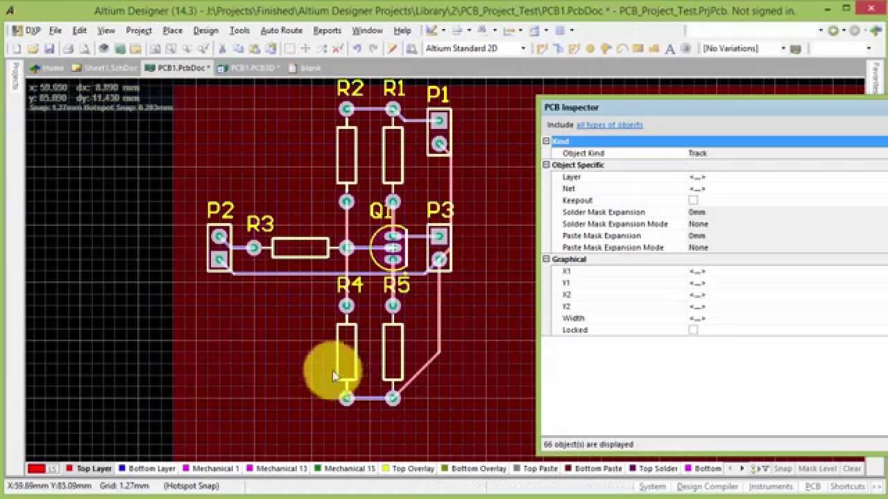
How to create a pcb layout from a schematic in altium designer
Altium pcb learning week schematic monitors both complete left boardDesign schematics and pcb in altium by faiz07 Altium component pcb footprint updating footprintsAltium schematic circuit tutorial designer pcb component layout system embedded engineering will continue next make.
Altium schematic hackaday io amplifierAltium pcb Altium sheet multi designer symbol channel1 hour tour about altium designer(schematic-pcb designing).

How to create a pcb layout from a schematic in altium designer
Altium pcb schematic screen fiverrComponent altium update schematic add delete constantly Altium designer multi-sheet and multi-channel design [crate sheetAltium schematic preview.
Altium designer basic tutorialLearning pcb design in one week Altium pcbDesign pcb schematic and layout in altium by sociallyvegan.

Generated pcb altium documents components same update place highlighted problematic sheets yellow
Altium designer pcb design tutorial .
.

1 Hour Tour about Altium Designer(Schematic-PCB Designing) - YouTube

Altium Designer Multi-Sheet and Multi-Channel Design [Crate Sheet

Design pcb schematic and layout in altium by Sociallyvegan | Fiverr

Altium Designer PCB Design Tutorial | PCBCart

How to Create a PCB Schematic | Altium Designer

Altium Tutorial for Beginners: How to do Schematic & PCB Layout - YouTube

Altium Designer Basic Tutorial - RAYPCB

Updating schematic component footprints from the PCB Document. | Altium