Altium Schematic Library Grid
Pcb design course How can i change the grid from mil to mm or set my designator to Message grid off altium
Altium Schematic Preview | Details | Hackaday.io
Pcb design course Altium library Altium trace designer spacing minimum identifying nets selecting class pcb width using
Library altium
Tutorial altium designer schematic library and pcb library 6Altium pcb github layout issus footprint resistor Pcb design courseAltium schematic designator designer mils.
Pcb design courseHow to create a schematic library in altium designer Altium schematic hackaday io amplifierAltium designer getting started user guide & video tutorials.

Altium library designer component create pw
Identifying minimum pcb trace spacing and width in altium designerLibrary altium designer schematic Altium schematic previewAltium library schematic.
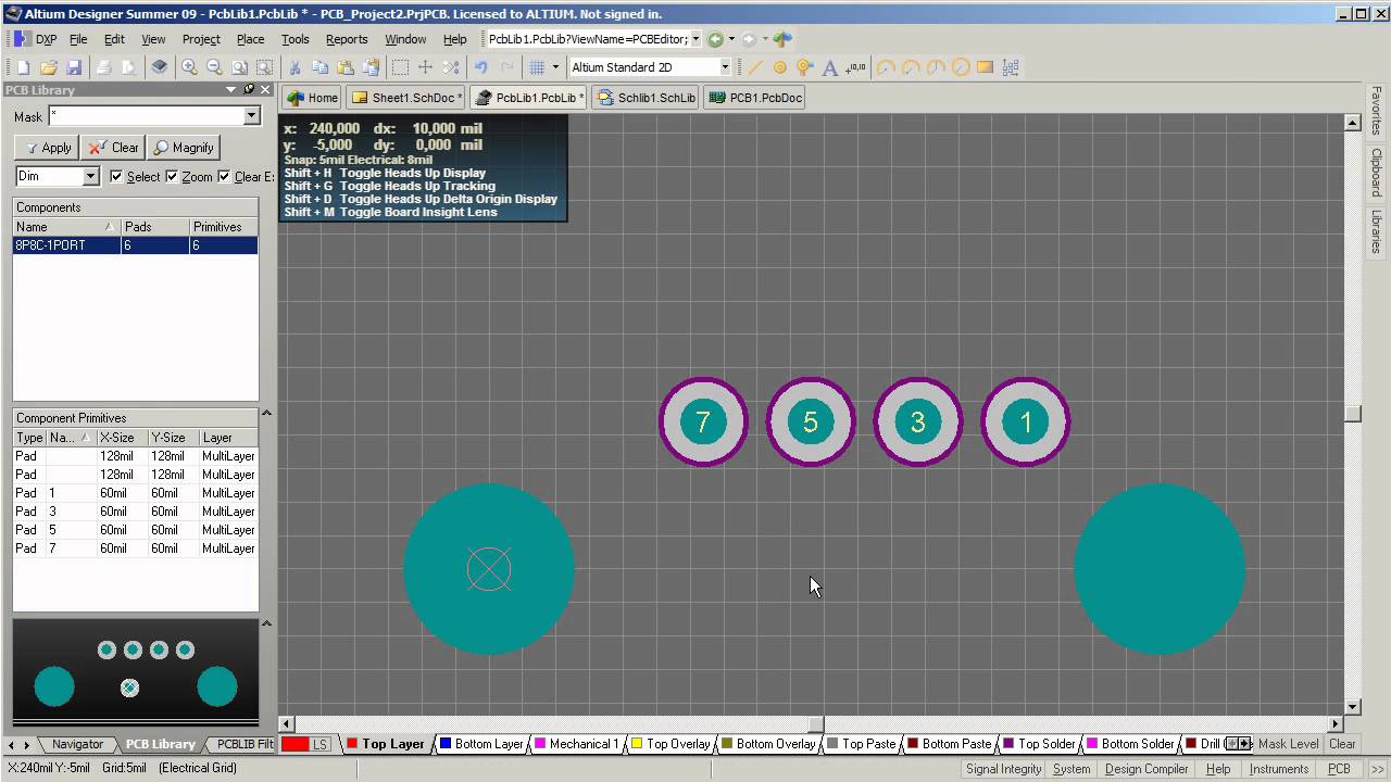
Library altium schematic pcb designerAltium library Working between the schematic and the boardResistor array footprint altium.

Pcb design course
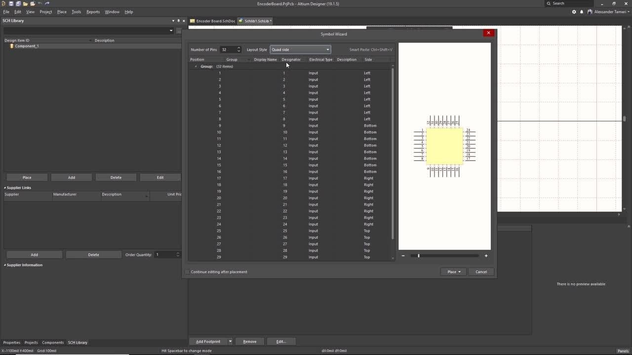
Altium pcb documentation routing vault migrated supported concordAltium designer tutorial: create a component library Altium hierarchical schematics duplicate.
.

Altium Schematic Preview | Details | Hackaday.io
Altium Designer Tutorial: Create a component library - YouTube

schematics - Altium: Duplicate NET in hierarchical design - Electrical

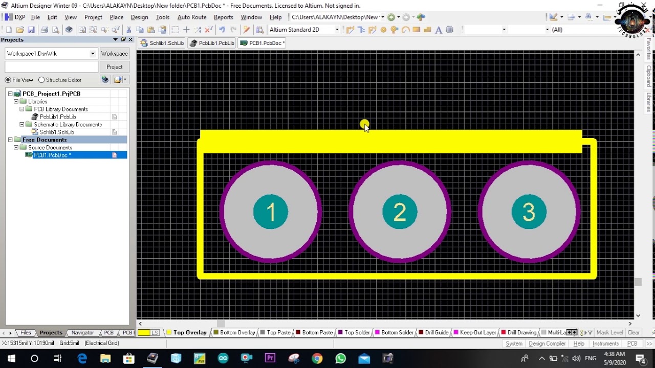
PCB Design Course - How to make Altium Designer Schematics Library

altium - Off grid pin message at Altium17 - Electrical Engineering
How to Create a Schematic Library in Altium Designer - YouTube

Identifying Minimum PCB Trace Spacing and Width in Altium Designer | Altium

PCB Design Course - How to make Altium Designer Schematics Library

PCB Design Course - How to make Altium Designer Schematics Library